
Microchips are everywhere in the modern world. They are the heart of every piece of technological equipment you can imagine. Technology companies have started to focus more and more on System-on-Chips (SoC) which combine all the functions of a device to a same chip. They are a key element in the technological development and can increase a company’s competitiveness significantly. By developing their own SoCs, companies can control their whole roadmap from silicon to web and differentiate by insourcing key expertise to themselves. All the top technology companies of the world have their own internal SoC technology development.
System-on-Chip development is a very special area to master. When it comes to tackling significant challenges in the industry no-one can make it alone: this requires global cooperation of companies and research organizations. Both need new talents and fresh thinking in order to succeed in the future world.
The disruptive potential of the SoC technology
System-on-Chip technology is the cornerstone of the EU’s digital transformation. Europe’s main competitors in the chip manufacturing are Asia and USA, but Europe is now significantly stepping up its game to increase technological sovereignty of the continent. EU Chips Act is a new initiative to increase European chip production capacity from 10% to 20% of the world market by 2030. IC manufacturing companies and EU will invest over 43 billion euros to support the Chips Act.
SoC development is also connected to the geopolitics. SoCs are critical for supply chains. Therefore, increasing skills in the SoC field will increase the security and decrease dependence on other countries. SoCs also have potential to increase data security.
Build your expertise in SoC design at Tampere University
Considering the development of the industry and where the world is going today, it is safe to say that there is an ever-growing demand for the System-on-Chip design experts in the technology field. The demand is already now very high. The IC experts specialized in SoC design have a lot of value in the job market today and companies are eager to hire all good candidates, whether they were in the beginning of their career or more experienced professionals. If you are good at what you do and most importantly eager to learn and genuinely interested, your chances to make a flourishing career in SoC development are high.
Tampere University has a unique combination of expertise areas covering the whole pipeline of SoC development from silicon to chip. In addition to the academic expertise and wide range of courses, Tampere University is experienced in the industry-academia cooperation and has connections with numerous companies as well as major technology vendors in the industry. Tampere has a long history and strong know-how in the field of SoC design, and Tampere University leads a pioneering System-on-Chip design co-creation project SoC Hub in which the university works together with the local companies. All these aspects considered, specializing in SoC design at Tampere University allows you to acquire a comprehensive view of the SoC industry.
The System-on-Chip design studies at Tampere University consist of all required expertise areas. The most important is digital design as all SoC projects involve it. Software engineering skills are essential to carry out modern digital design, because the “HW” is expressed in Hardware Description Languages (HDL) and the process involves a lot of scripting. Supporting expertise areas are embedded systems and analog circuits and microelectronics, which is required for foundational building blocks like high-speed clocks and gigabit-grade off-chip connections. However, such special blocks are often reused, and no new design is needed in a new project. Electronics, production and testing are required since most chips need Printed Circuit Boards (PCB) for testing, as well as lab infrastructure. Wireless communication, signal processing and math are very useful for bringing application knowledge to the SoC requirements.
At Tampere University, you can take studies that are related to System-on-Chip design if you are an information technology or electrical engineering student and study embedded systems as your major. First, we will have a look at what is a System-on-Chip and how it is designed.
What is a System-on-Chip?
Just as its name would suggest: a system that is integrated on a single chip. Since more and more can be integrated, the system consists of subsystems, which in turn consist of Intellectual Property (IP) Blocks that are the basic building blocks. A processor core is an IP block, but with all its on-chip memories and peripherals it forms a processor subsystem. As an example, SoC Hub’s first chip “Ballast” includes three RISC-V subsystems, one DSP subsystem, a machine learning accelerator subsystem (NVDLA), and an Ethernet subsystem. The subsystems are interconnected via on-chip buses (AXI), and external interfaces are chip to chip (C2C) for other systems, Ethernet and various peripheral IOs. Clocking (PLL) is distributed and forms domains with different speeds.
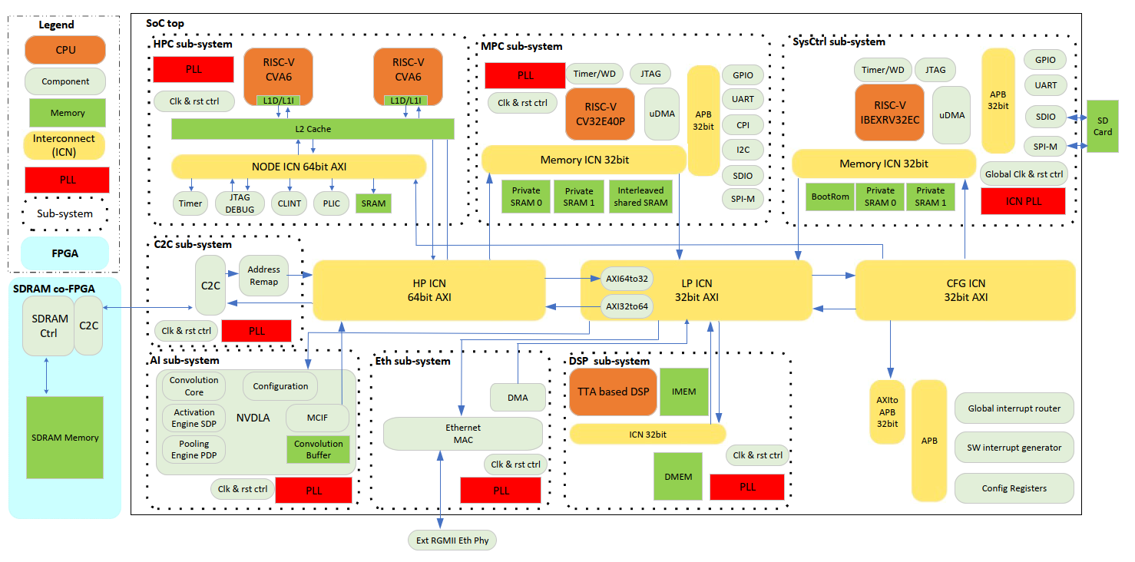
Ballast is intended for general-purpose IoT/Edge computing. Typically, SoC expertise can be agnostic to any application and the designer can utilize the same skills in many projects. However, subsystems and IP blocks can be highly optimized for a specific purpose, which requires also understanding of the application.
How to design a System-on-Chip?
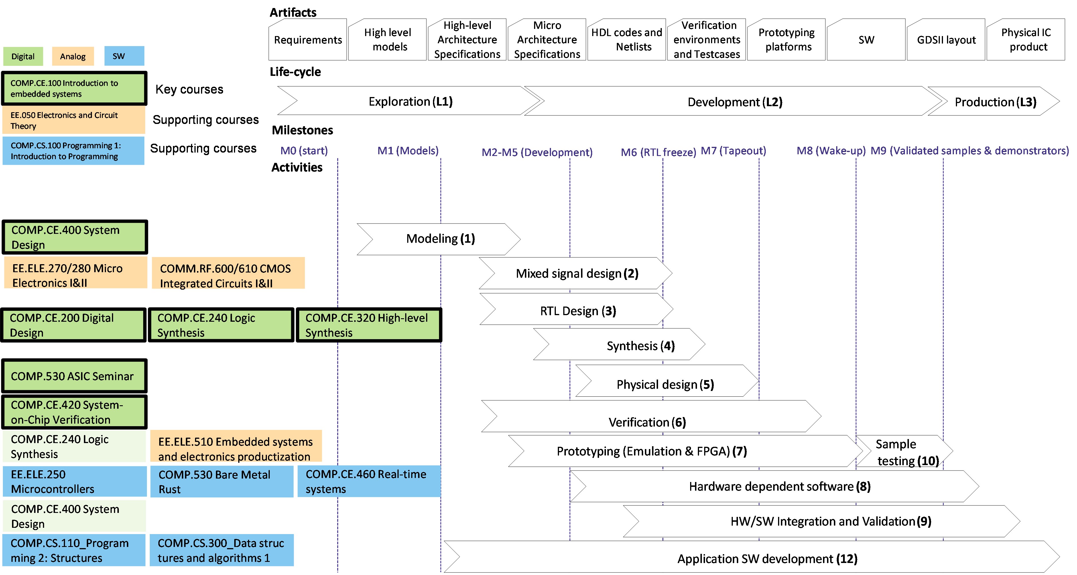
The main phases of the System-on-Chip design flow are Exploration, Development and Production according to the life cycle of the product. The biggest decisions are made first when the requirements are set and explored against available technologies, scheduling and costs. The development includes hardware and software design as well as their verification and integration. After acceptable chip samples and stable software, the production can start in volume. The work is iterative in nature, but many tasks must be conducted in strict order within each phase.
Infrastructure
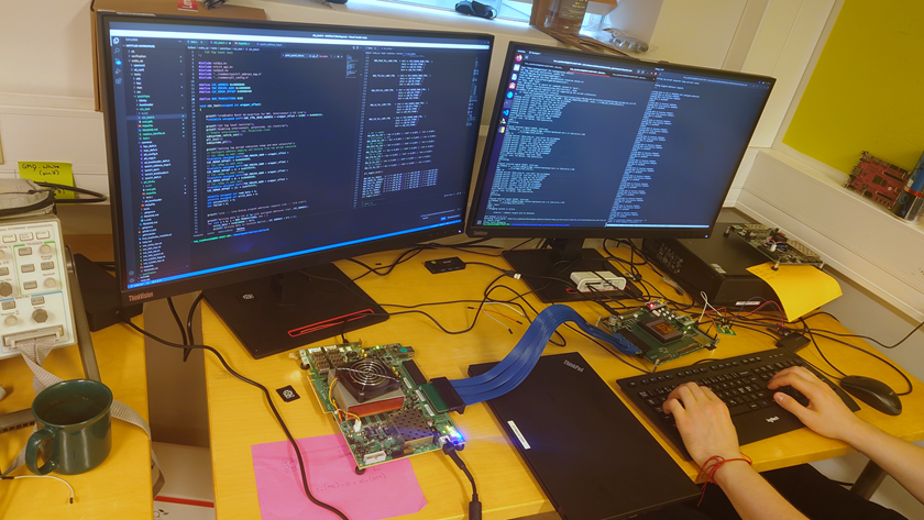
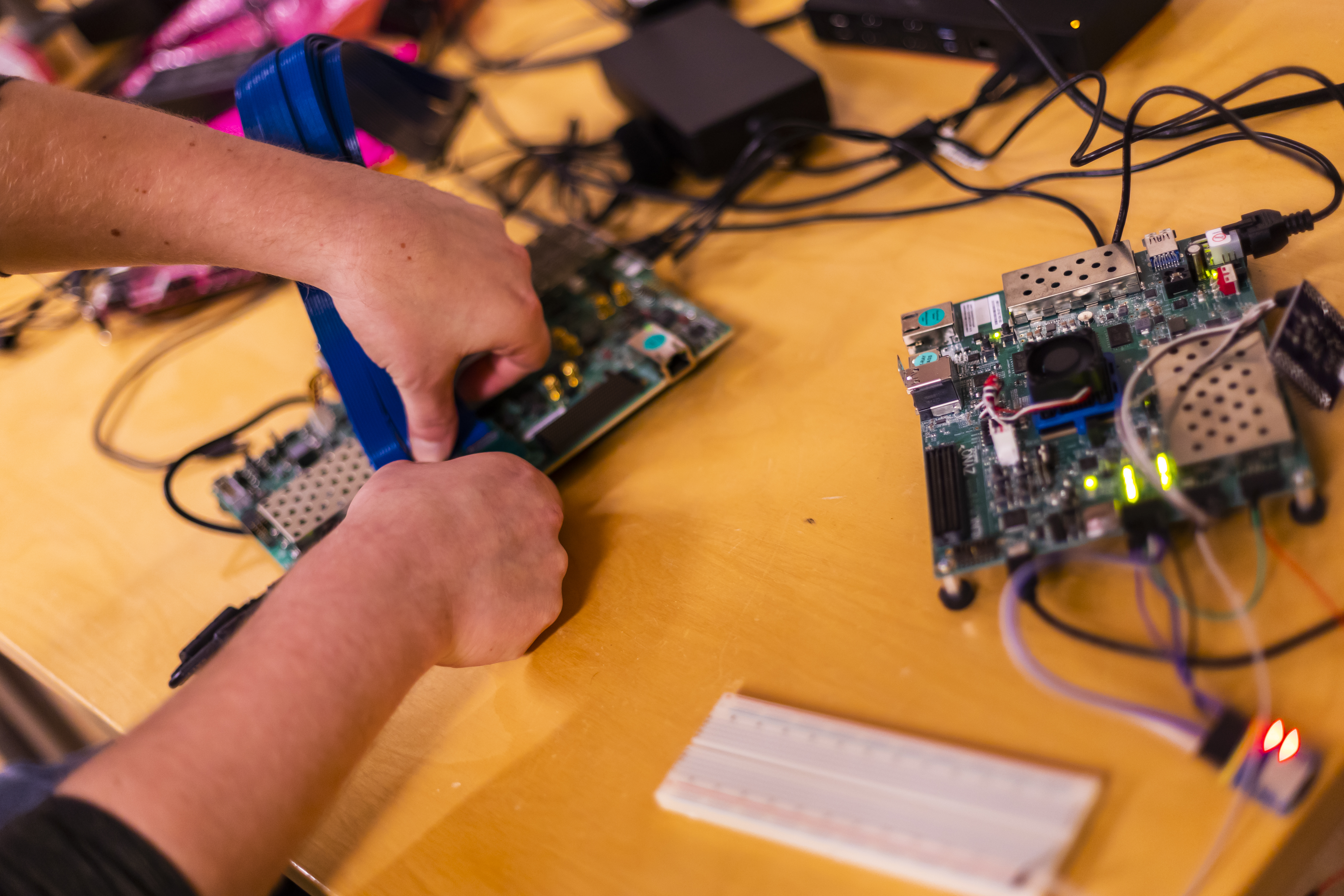
SoC design requires setting up extensive server capacity for computing and storage, design tools, design files and data repositories, access to ASIC technology libraries, and physical laboratories and devices for testing the chips. For example, SoC Hub servers have 144 CPU cores @ 4 GHz and 4,5 TB RAM. Our design tools, libraries, and work files consume 14 TB of disk in total.
The legal agreements and rights management are crucial in addition to the management of the design process and manufacturing supply chain. Most often the design requires third party IP blocks, for example on-chip memory that would be very laborious to design from scratch. For this reason, the design environment also supports integration of building blocks from different sources.
Artifacts
The design flow creates concrete tangible documents, materials, files and supporting devices that we call design artifacts. For the Exploration (L1) they are requirements, high-level architectural specification, high-level models (HLM) and micro-architectural specifications. The typical Development (L2) artifacts consist of hardware description language (HDL) codes synthesized to machine-readable circuit description netlists and eventually physical transistor layout descriptions in GDSII format for chip production. Supporting artifacts include test cases and data, virtual verification environments and physical prototyping platform designs for example in FPGAs. Software has its own artifacts, as well as information exchange between hardware and software. The production phase (L3) includes the manufactured chip itself, chip package, production qualification and chip samples testing printed circuit boards or measurement equipment pin beds.
Milestones
Milestones (M0-M9) show the readiness of the SoC during the design flow. Milestones are used to synchronize the work between the development activities and as quality control points.
The Development (L2) includes several milestones (M2-M5) which reflect the design maturity from incomplete draft models to verified ones. RTL Freeze (M6) means that the architecture (for example inputs and outputs, subsystems, IP blocks and clock domains) cannot be changed, and very extensive work towards Tape-out (M7) starts. This is the point when the chip goes into physical production and the HW design stops. Tape-out is a historical term which originates from the time when the huge amount of design data for production was transferred with big magnetic tapes. After fabrication the chip is woken up (M8) which means the elementary HW functions like clocking, reset, and processor booting are working. After this the chip can be handed over to more software focused testing and developing application demonstrators. At this point the chip is ready, and it includes a board support package (BSP) for low-level SW development and most often also a software development kit (SDK) for application programming.
Abstractions
SoC design requires several levels of design abstraction. The highest-level addresses pure functionality in which timing is not considered but only correct input and output data and behavior. The timing is included first at coarse resolution at transaction-level model (TLM) and finally at clock cycle accurate level. The lower the timing abstraction, the longer the simulation runs take. For example, booting Linux on cycle accurate processor model can take days of simulation time. It is not possible to simulate the same at any reasonable time using transistor level models. Therefore, higher abstractions are applied to save development time and effort.
How are the courses connected to the real-life SoC development?
Tampere University teaches chip design techniques on various courses. Next, we will tell how our courses are related to the SoC design flow with the help of the activities depicted in the diagram.
Activities
The real SoC design work is done in activities. The arrows in the SoC design flow diagram depict the mutual timing and order, and key mission of each activity. Within each activity there are tens of detailed tasks.

SoC development activities start with modeling, which is taught at System Design course. The purpose of modeling is to make right decisions, because the overall flow is complex and big changes later are costly. In this phase, the requirements for the system are defined and explored with abstract system models in SystemC that can be executed, simulated, and analyzed. The system includes the large entity consisting of the architecture, modules, and interfaces both for HW and SW. Parts of the abstract system model can be generated for implementation, for example automatically getting Verilog HDL code from the IP-XACT models.
Next starts the detailed HW design. The most important is digital HW design that is carried out by writing HDL code at register transfer level (RTL) abstraction, i.e. RTL design. In addition, scripts are used to generate and manipulate the codebase, and integrate IP blocks from third party vendors. RTL design resembles much more software programming than circuit design in mixed signal design. Both analog and digital design can be executed in parallel.
The mixed signal design is often outsourced from IP vendors. When mixed signal design is included in the project, functionality on analog microelectronics at the border of analog and digital HW design is created. For example, phase-locked loop (PLL) is required to generate GHz level clock signals inside the chip, or HDMI display port requires very high-speed transceiver circuits. This requires mastering transistor level design about which you will learn the basics at the Micro Electronics I and II and Integrated Circuits I and II courses. The design is carried out with electronic design automation (EDA) tools with drawing circuit diagrams.

Synthesis is a highly automated task that creates the low-level structure of gates, registers and connections either for FPGA or ASIC technology. The courses Digital Design, Logic Synthesis and High-Level Synthesis (HLS) cover both RTL design and synthesis. The Digital Design course educates basics of gate networks, state machines, arithmetic units, and digital system architectures. Logic Synthesis trains digital design using HDL language at RTL level abstraction (VHDL). For new hardware developers, this is the most important skill, and knowledge in this area has traditionally been very valued among companies. Furthermore, High-Level Synthesis (HLS) course considers how RTL level code can be automatically generated from C or C++ language, which increases design productivity.
Physical design means creating the transistor layout on the silicon die. Its input is netlist from the synthesis phase, and it creates the placement and routing of the transistors. However, the designer usually sees only standard cells that are composed of the transistors like gates, registers, memories, interconnects and other blocks. Only full-custom design exposes the single transistors to the designer. Our seminar course on Digital ASIC Backend addresses all the steps required for tape-out ready chip design.
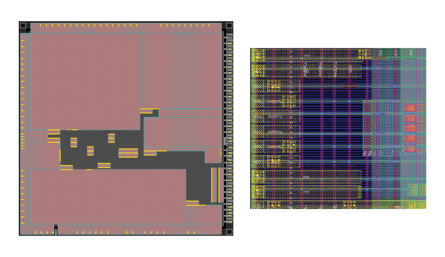
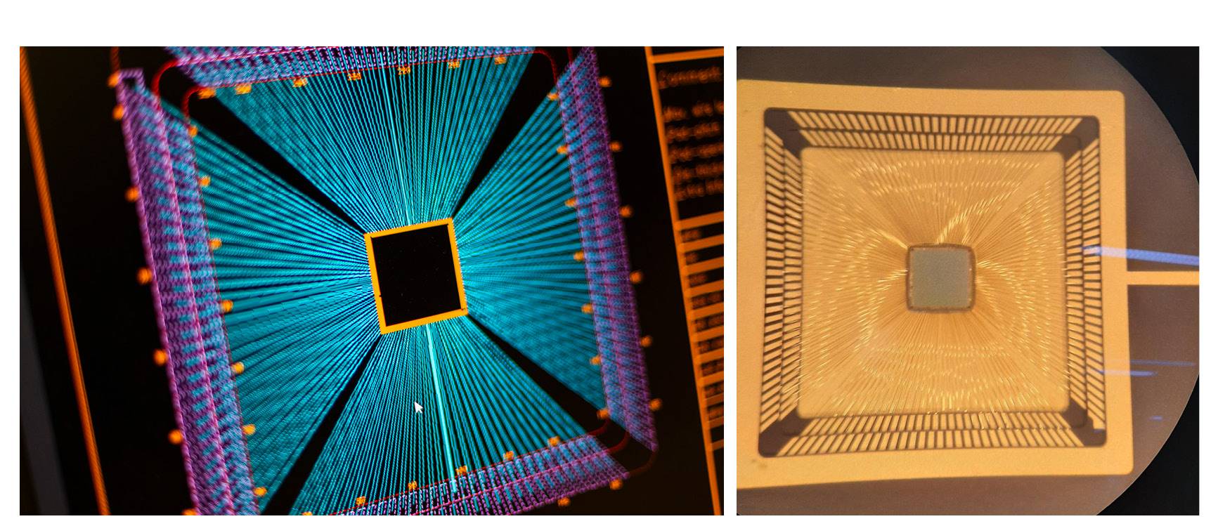
Packaging is required to attach the manufactured silicon die to the rest of the electronic product like a printed circuit board. Package design starts when the layout and type of IO pads are frozen in the physical design. The tasks include the selection of the package type, internal routing design inside the package. The die is usually attached to the package by wire bonding or directly by die surface called flip-chip.
Verification is a process of ensuring that the SoC design meets its specification, and it is usually carried out as simulations. This is taught at the System-on-Chip Verification course. We use Universal Verification Methodology (UVM) standard as the backbone, as well as SystemVerilog language.
Prototyping refers here to physical testing of the chip. In prototyping, the RTL description of the chip is synthesized to the programmable FPGA, which then emulates the chip. The focus is on functionality, because the timing and clock speeds usually differ between the final SoC and FPGA. Prototyping is addressed in many of our courses that use FPGA as the exercise platform.
Sample testing takes place when the packetized dies have arrived from manufacturing. It includes unpacking the chips, assembling them to a custom-made printed circuit board (PCB) and start testing by electrical checks. After this begins the actual wake-up, in which power levels and clocks are started in sequences and JTAG-based checking of all internal blocks and subsystems is carried out. Our Embedded Systems and Electronics Productization course teaches how to create PCBs.
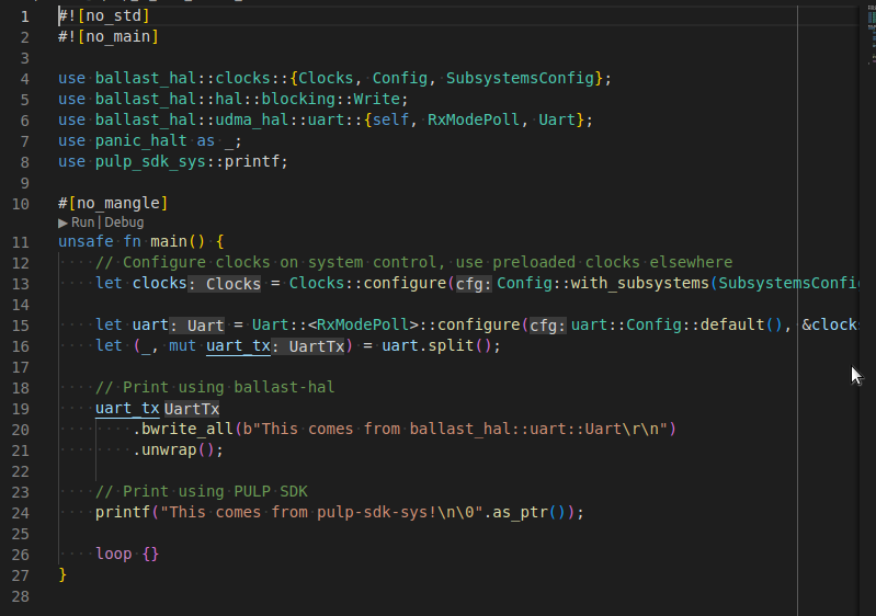
Software interacts with the hardware by reading and writing HW registers at the lowest level. The memory maps required for SW are generated from the HW design data, for example IP-XACT models. So-called hardware-dependent software is then created that abstract low-level details from the programmer. The set of libraries and functions is often called board support package (BSP), which in turn is required for a software development kit (SDK) for the application programmer. We teach how to create programs right on top of HW in our Bare Metal Rust seminar, and how to build Linux and create specific HW device drivers for Linux in our Real-Time Systems course.
One of the final steps in SoC design is HW/SW integration and validation. System Design course wraps up both the digital design and programming courses. As an exercise it creates a complete HEVC video encoder, in which part of the functionality is executed in processor and part in custom HW design under Linux.
Finally, when the chip samples are tested, the handover from HW implementation to application software development takes place. Our extensive set of Software Engineering Courses and Software Development are recommended for these tasks.
Courses related to SoC design at Tampere University
ESSENTIAL COURSES
Digital design:
– COMP.CE.100 Introduction to embedded systems
– COMP.CE.200 Digital Design
– COMP.CE.240 Logic Synthesis
– COMP.CE.320 High-level Synthesis
– COMP.CE.400 System Design
– COMP.CE.420 System-on-Chip Verification
– COMP.530 Post-Graduate Course on Computing: ASIC Seminar
Computer engineering:
– COMP.CE.130 Computer Architecture
Embedded systems:
– EE.ELE.250 Microcontrollers
Software engineering:
– COMP.CS.100 Programming 1: Introduction to Programming
– COMP.CS.110 Programming 2: Structures
– COMP.CS.300 Data structures and algorithms 1
– COMP.SE.100 Introduction to Software Engineering
– COMP.SE.110 Ohjelmistojen suunnittelu / Software Design
– COMP.SE.121 Software Product and Process Management
SUPPORTING COURSES
Microelectronics:
– EE.050 Electronics and Circuit Theory
– EE.ELE.270 Micro Electronics I
– EE.ELE.280 Micro Electronics II
– COMM.RF.600 CMOS Integrated Circuits I
– COMM.RF.610 CMOS Integrated Circuits II
– COMM.RF.700 RF Circuit Design
– COMM.RF.430 Transmission lines and Waveguides
Electronics:
– EE.020 Elektroniikan perusteet (FI)
– EE.ELE.210 Transistorit ja vahvistinpiirit
– EE.ELE.200 Elektroniikkalaitteen tuotesuunnittelu
– COMM.RF.200 Johdatus RF-elektroniikkaan
– EE.ELE.450 Semiconductor Device Physics
– EE.ELE.510 Embedded systems and electronics productization
Computer engineering:
– COMP.CE.260 Computer Arithmetic
– COMP.CE.350 Parallel Computing
– COMP.CE.460 Real-time systems
– COMP.530 Post-Graduate Course on Computing: Bare Metal Rust
– COMP.CE.430 Computer Graphics
Embedded Systems:
– EE.ELE.500 Mikrokontrollerijärjestelmät (FI)
– EE.ELE.510 Embedded systems and electronics productization
– EE.ELE.520 Verkotetut sulautetut järjestelmät (FI)
Software engineering:
– COMP.CS.310 Concurrency
– COMP.CS.410 Operating Systems
Math:
– MATH.MA.210 Discrete mathematics
– MATH.APP.27 Algorithms for graphs
– MATH.APP.460 Numeerical analysis
– COMP.CS.330 Automata and formal languages
– COMP.CS.420 Introduction to formal specification
– MATH.MA.610 Graafiteoria (FI)
Wireless communications:
– COMM.100 Basic Course on Communications Engineering
– COMM.SYS.200 Basic Course on Wireless Communications
– COMM.SYS.300 Communication Theory
– COMM.SYS.400 Digital Communication
– COMM.SYS.450 Multicarrier and Multiantenna Techniques
– COMM.SYS.700 5G Mobile Communications
– COMM.SYS.800 Communication Systems Laboratory Course
– COMM.SYS.650 Software-Defined Radio Platforms
– COMM.SYS.900 Advanced Course in Digital Communication
– COMM.SYS.660 Radio Architectures and Signal Processing
Signal processing:
– COMP.SGN.100 Introduction to Signal Processing
– DATA.ML.100 Introduction to Pattern Recognition and Machine Learning
– COMP.SGN.110 Introduction to Image and Video Processing
– COMP.SGN.200 Advanced Signal Processing